Fundamental Structure of a MOSFET
The MOSFET is a MOS structure with two contacts on each side.

> No current flow
By controlling the gate, we can turn on and turn off the channel. If the gate is turned on, electrons appear in the channel region.
> The thin electron layer (the channel) connects source and drain.
 connects source and drain.")
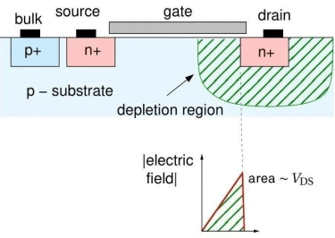
Blocking Mode
In blocking operation (gate turned off, no channel) there is a depletion region between drain and p-substrate (which is connected to source via bulk).
Requirements for High Blocking Voltages
High electric fields can cause avalance. However, a large area is required for high blocking voltages. Further, the depletion region must not extend into source to avoid punch-through currents.
> Need a wide depletion region

Impact on On-State Resistance
However, a wide MOSFET also has a long channel:

This increases the on-state resistance Rpson.
Fortunately, there are better concepts.
Drain-Extended MOSFET
We can shorten the channel by introducing a lowly doped n- region.

> Decreased Rpson
In blocking mode, however, the depletion region extends through the lowly doped n- region.

> Wide depletion region, high breakdown voltage
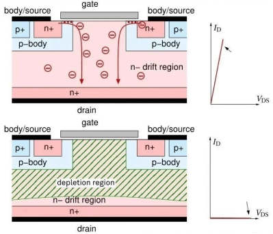
Vertical DMoS
Further optimization by increasing the drain contact area:

Note: The n+ layer is much thicker than shown here. (Fabrication starts with a thick highly n+-doped wafer, on which the lowly doped n- drift region is deposited.)
On-and Off-State
Saturation
At a certain drain-source voltage the depletion regions between p-body and n-drift regions merge (pinch-off). Then, the current does not increase anymore: saturation
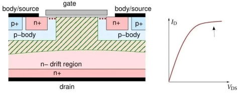
This also shields the gate from high voltages.
> Gate oxide can be thin everywhere (for vertical DMOS)
Trench MOSFET
Today, Trench MOSFETs are commonly used.
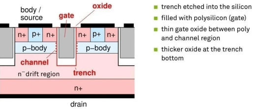
> No JFET effect anymore (pinch-off by adjacent p-bodies in planar MOSFETs)
> Higher channel density per area possible (channel now not limited by silicon surface. Trench surface can be larger.)
Capacitances
MOSFETs are unipolar devices (apart from the body diode) Switching speed is mostly determined by charging and discharging the parasitic capacitances.

Some depend on the depletion region width, i.e. on VDS.
Dependence on the operating point:
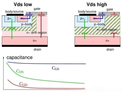
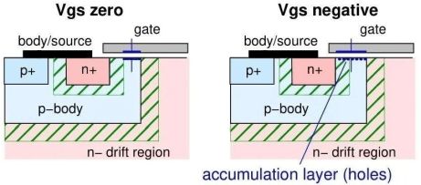
Note that for negative gate-source voltages, the input capacitance (most notably CGs increases further. This is because if VGS becomes negative, accumulation occurs in the p-body.