

A typical discrete driver circuit's core task is: to receive weak signals from the control chip (such as MCU, PWM chip), and amplify them into a current source and current sink that can quickly and powerfully drive the gate of the IGBT. The main design considerations are similar to those of integrated circuit drivers, but all functions need to be implemented using discrete components:
- Providing sufficient driving current: to achieve rapid charging and discharging of the IGBT gate capacitance (Cge, Cgc), shortening the switching time and reducing switching losses.
- Providing appropriate driving voltage: typically +15V ±10% for turn-on and -5V to -15V for turn-off. Negative voltage turn-off can enhance anti-interference ability and prevent Miller capacitance effect-induced misconduction.
- Achieving fast switching speed: requiring the push-pull output stage to have very low output impedance.
- Necessary protection functions: such as gate resistor selection, gate clamping, active Miller clamping, etc. (more complex protections such as saturation detection are very difficult to implement).
Therefore, different types of driver circuits that are driven by different discrete components have been derived:
Driver circuit (voltage type)
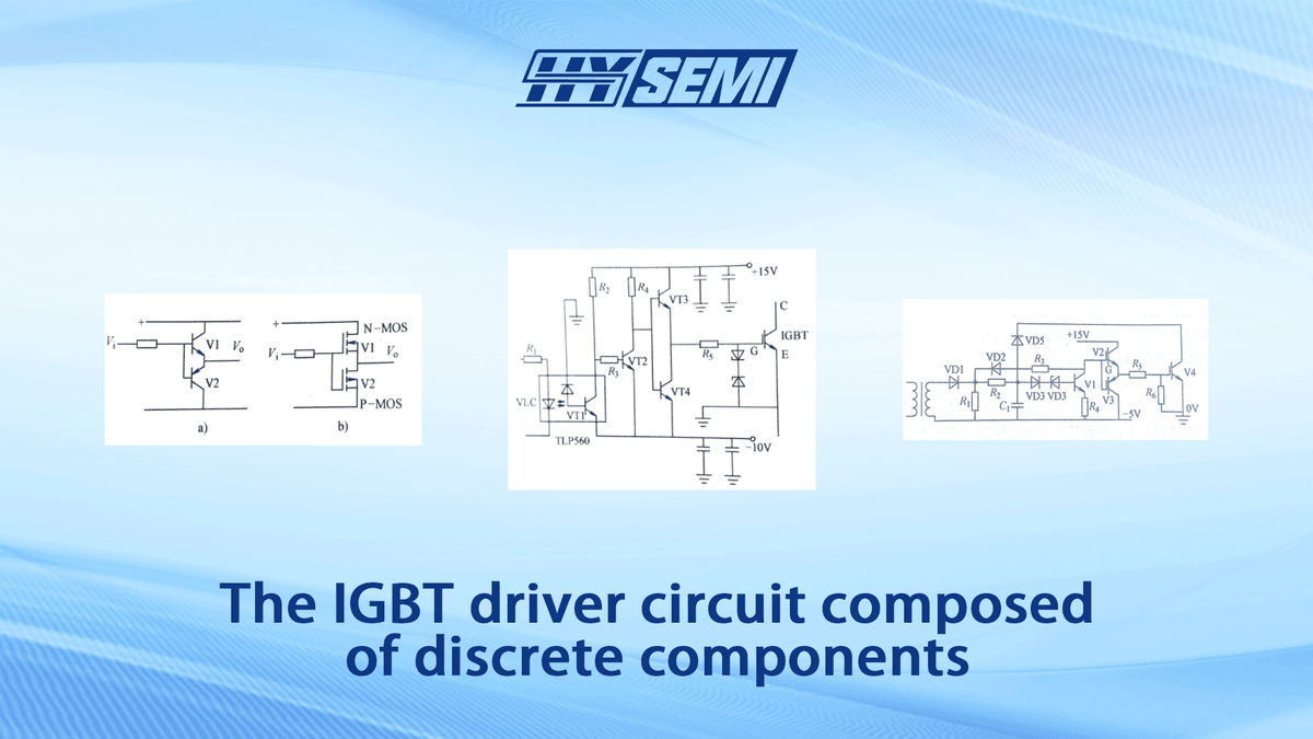
The driver circuit shown in Figure 1a is suitable for driving low-frequency small-power IGBT. When the control signal Vi is high, Vl conducts, and the output Vo corresponds to the control's conducting IGBT (IGBT); when the control signal Vi is low, V2 conducts, and the output Vo corresponds to the control's turned-off IGBT (IGBT).
")
Figure 1 Drive Circuit (Voltage Type)
The drive circuit shown in Figure 1b is composed of field-effect transistors to form a push-pull circuit, and its working principle is the same as that in Figure 1a. This circuit can achieve a peak driving current of over 10A at high frequencies and is suitable for large-power IGBT devices.
Drive and Protection Integrated Circuit
Figure 2 shows the drive and protection integrated circuit, which is suitable for driving low-frequency and low-power IGBT. If the bipolar NPN and PNP transistors are replaced with N-channel and P-channel high-power field transistors, a high-frequency and high-current driver can be formed.

Figure 2 Integrated Drive and Protection Circuit
In the integrated drive and protection circuit shown in Figure 2, instead of using an optocoupler for signal isolation, a magnetic ring transformer is used to couple the square wave signal. Since the speed of the optocoupler is not fast enough and there is a delay in the rising and falling wave along of the optocoupler, using the transformer for transmission can obtain a steep rising and falling wave along, with almost no transmission delay. This circuit is suitable for driving high-frequency and high-power IGBT devices. This circuit has a fast drive speed, fast overcurrent protection action, and is a relatively ideal integrated drive and protection practical IGBT driving circuit.
Discrete Component-Based IGBT Drive Circuit
The drive circuit shown in Figure 4 is an IGBT drive circuit constructed using discrete components such as optocouplers. When the input control signal is applied, the optocoupler VLC conducts, transistor V2 is cut off, and transistor V3 conducts to output a +15V driving voltage. When the input control signal is zero, VLC is cut off, V2 and V3 are conducting, and a -10V voltage is output. The +15V and -10V power supplies should be close to the drive circuit. The leads from the output end of the drive circuit and the power ground terminal to the gate and emitter of the IGBT should use twisted-pair wires, and the length should preferably be no more than 0.5m.

Figure 4: IGBT driver circuit composed of discrete components
When designing the IGBT driver circuit, the following points should be noted:
- The gate withstand voltage of IGBT is generally around ±20V. Therefore, a gate overvoltage protection circuit should be provided at the output end of the driver circuit. The common practice is to parallel a voltage stabilizing diode or resistor across the gate. The disadvantage of paralleling a voltage stabilizing diode is that it increases the equivalent input capacitance Cin, thereby affecting the switching speed. The disadvantage of paralleling a resistor is that it reduces the input impedance and increases the driving current. The choice should be made based on the actual needs.
- Although the driving power required by IGBT is very small, due to the input capacitance Cin of MOSFET, charging and discharging of the capacitance are required during the switching process. Therefore, the output current of the driver circuit should be large enough. Assuming that during the conduction drive, the MOSFET input capacitance Cin is linearly charged within the rising time tr, the driving current is IGE = Cin × VGS / tr, where tr can be taken as 2.2RCin, and R is the input loop resistance.
- To reliably turn off the IGBT and prevent the lock-in effect, a negative bias voltage should be applied to the gate. Therefore, a dual power supply should be used to power the driver circuit.
For low-power, low-cost, and non-critical applications, a simple discrete driver circuit is a feasible option. For medium-high power or applications with high reliability requiremen, SHYSEMI strongly recommends using dedicated IGBT driver chips. Because the driver chip integrates push-pull output, isolation, under-voltage protection, undervoltage detection, and active Miller clamping functions, it greatly simplifies the design at a significantly reduced cost and significantly improves the reliability and safety of the system. This is usually a more cost-effective choice than the discrete solution.