

Introduction: The Chip Didn't Change—the Package Is the Bottleneck
Take the same SiC die, change only the package, and switching loss can differ by 20–35% while junction temperature shifts by ten-odd degrees—the chip is identical, yet the bottleneck is the package. Many engineers blame "wrong device selection" for performance problems when the real issue is wrong package selection: a plain TO247-3L SiC running a 500 kHz converter lets package parasitics eat the die's own advantage.
One sentence: the package dictates the die's outward current path, parasitic parameters, thermal route, and interface thermal resistance—directly driving conduction loss, switching loss, and the thermal-design choice. This article splits into two parts—how packaging affects loss, and how it affects thermal design—then compares typical packages.
Pain hook: You think efficiency is low because the chip isn't good enough, but parasitics and thermal resistance in the package are quietly "stealing" your performance and lifetime.
Basics: Two Concepts to Set First
- Loss budget: conduction loss + switching loss + drive loss + parasitic loss;
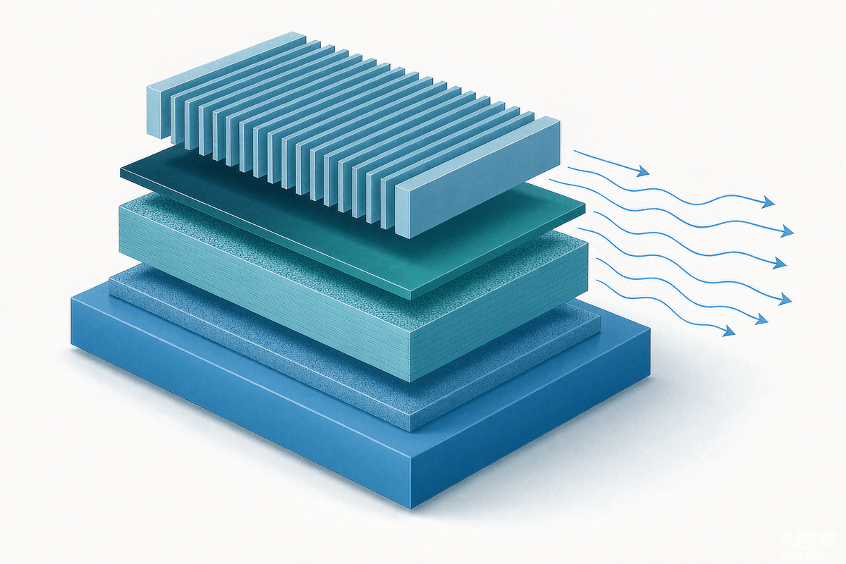
- Thermal chain: junction → solder / silver-sinter layer → substrate (DBC) → TIM → heatsink → ambient; every layer is a thermal resistance.
1. How Packaging Affects Loss
1.1 Internal interconnect parasitics: inductance & resistance
Bond wires, copper frames, leads, and busbars inside the package introduce parasitic Ls and Rs:
- Parasitic resistance Rs adds directly in series with the die; at high current it creates extra conduction loss;
- Parasitic inductance Ls generates voltage spikes during switching (high di/dt), raising voltage-stress margin requirements, adding ringing, and increasing switching loss and EMI.
SiC devices have far higher di/dt than silicon IGBT/MOS, so they are extremely sensitive to package parasitic inductance.
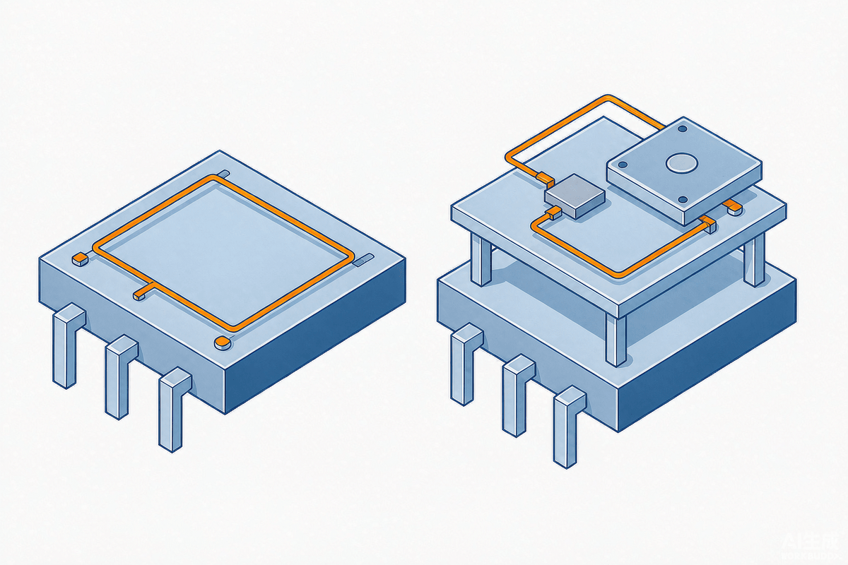
Example: the TO-247 discrete uses traditional Al wire-bonding + long leads, with parasitic inductance ~10–15 nH; in high-frequency LLC / QR flyback or onboard OBC this causes large switching spikes and forces RC snubbers, adding loss. By contrast, SiC HPD (leadless / planar) packages and Kelvin-source TO247-4L break out the drive source separately, decoupling the power and gate loops to cut power-loop inductance—switching loss drops markedly at the same frequency, the go-to for high-frequency supplies.
Comparison: same SiC MOS die, TO247-3L vs TO247-4L at 800V / 20A switching—the 4L package's switching loss is 20–35% lower.
1.2 Current capability and sharing (multi-die parallel modules)
In parallel modules (IPM, IGBT module, multi-die SiC module), uneven internal copper routing and bond-wire lengths cause current imbalance: some dies overload, loss concentrates in a single die, overall loss rises, and local overheating occurs.
Example: a plain IPM with Al wire-bonded parallel IGBTs shows large per-die current deviation under high current if routing is asymmetric; advanced modules use DCB direct-copper-bonding, large copper busbars, and silver sintering for better sharing and higher parallel utilization—no single-die "overload heating."
1.3 Internal material resistance and bonding
Al wire-bond vs Cu wire-bond vs Ag sinter:
- Al wire has high resistivity and limited cross-section → more loss at high current;
- Cu wire / Cu strap / Ag sinter conduct better, lower series resistance → lower conduction loss.
Example: industrial high-power IGBT modules—old Al wire-bond vs new Cu strap at the same die spec show a slightly lower module Vce(sat) and less loss under sustained high current.
2. How Packaging Affects Thermal Design (Rθ, path, capacity, distribution)
Key thermal metrics: Rθ(j-c) junction-to-case and Rθ(c-h) case-to-heatsink; the package decides the thermal path.
2.1 Thermal path: single-sided vs double-sided cooling
- Single-sided (most TO packages, conventional DBC modules): heat only goes down through the die to substrate and case; the top is molding compound with poor thermal conductivity, almost no cooling.
- Double-sided: metal interconnect top and bottom, both attach to heatsinks → Rθ(j-c) drops sharply.
Example: automotive SiC power module with double-sided cooling shows >40% lower junction-to-case resistance at the same die—lower junction temperature at equal loss, or higher allowable output; but heatsink structure, insulation, and cost rise significantly.
2.2 Substrate material (DBC, AMB, AlN)
The die is soldered to the substrate, the key thermal-spreading layer:
- Al₂O₃ DBC: cheap, moderate thermal conductivity (~24 W/mK);
- AlN DBC: high conductivity (~170–230 W/mK);
- AMB (active metal brazing): Si₃N₄ substrate, high conductivity + high strength, suited to SiC high-temperature and thermal-cycling scenarios.
Example: same SiC die—alumina DBC module runs hot at full load and must be derated; switching to Si₃N₄ AMB improves spreading and thermal-cycling life, ideal for EV traction, at a much higher substrate cost.
Molding compound itself conducts poorly, so TO-package dies can only shed heat through the copper frame; molding only insulates and does not cool.
2.3 Interface layers and interface resistance
Every interface on the thermal path (solder, sinter, substrate solder, TIM grease) stacks resistance:
- Solder: medium interface resistance, prone to fatigue cracking under long thermal cycling;
- Silver sinter: low porosity, good conduction, far lower interface resistance than solder, suited to high-temperature SiC (junction up to 175℃ / 200℃).
Example: traditional TO247 die soldered to copper frame vs high-end SiC discrete with Ag sinter—same power, ~10–25℃ lower junction.
2.4 Package shell, contact flatness, insulation needs
- TO package: small bottom copper flange, limited effective heatsink contact area; poor torque control warps the part and makes TIM thickness uneven, spiking local resistance;
- Module package: flat metal baseplate, large contact area, easier even heating; but the insulation requirement between baseplate and power terminals trades off—thicker insulation layer = higher voltage rating but worse thermal conduction.
Example: an IPM integrates DBC, IGBT, FRD, driver, and protection with a unified baseplate—simpler system thermal design, but the package is fixed so you cannot freely change the substrate or go double-sided; the loss ceiling is locked by the package.
2.5 Thermal capacity and transient impedance (pulsed load)
The copper and substrate mass set thermal capacity. Motors and welders are pulsed loads (intermittent high current), so watch transient impedance Zth:
- Large module substrates have high mass → slow junction-temperature rise under short peak loss;
- Small packages (SOT-227, DPAK) have tiny thermal mass → even at low average loss, short pulses spike the junction.
Example: same MOS die, DPAK (TO252) vs TO247 under sustained DC loss is similar, but in a welder peak-pulse scenario the DPAK junction shoots up and easily suffers thermal breakdown.
3. Comparison Case
Same SiC MOS die in three packages—loss & thermal differences:
- TO247-3L (3-pin): high parasitic inductance → high switching loss, poor at high frequency; single-sided, small copper flange, Rθ(j-c) ≈ 0.8–1.2 ℃/W; for low-frequency, small/medium-power supplies.
- TO247-4L (Kelvin source): decoupled power/gate loops, low Ls → markedly lower switching loss; thermal resistance similar to 3L; preferred for high-frequency LLC, OBC, energy-storage converters.
- SiC AMB DBC power module: internal copper busbar, very low parasitic inductance, good multi-die sharing; Si₃N₄ substrate + Ag sinter, very low Rθ(j-c); lowest loss, strongest cooling; but costly, needs water-cooling/thick heatsink, plus insulation and voltage-balancing considerations.
4. One Key Trade-off
Package design is always a compromise:
- Want low switching loss → cut parasitic inductance: planar interconnect, Kelvin, short busbar;
- Want low thermal resistance → double-sided cooling, high-conductivity substrate, Ag sinter, larger area;
- Cost: bigger size, pricier process, harder insulation, changed EMI structure.
Conversely, if package selection is wrong, even a great die becomes bottlenecked by loss and thermal. Put a plain TO247-3L SiC into a 500 kHz converter and package parasitics eat the die's advantage.
5. FAQ
Q: Why does packaging affect switching loss?
A: The package's leads, pins, and busbars introduce parasitic inductance; under high di/dt switching this creates voltage spikes and ringing that raise voltage-stress margin needs and add switching loss and EMI. SiC devices are especially sensitive to parasitic inductance.
Q: What does a Kelvin source (TO247-4L) do?
A: It breaks out the gate-loop source separately, decoupling the power and gate loops to reduce power-path parasitic inductance. At 800V/20A the 4L's switching loss is 20–35% lower than the 3L's—the first choice for high-frequency supplies.
Q: How to choose between DBC and AMB substrates?
A: DBC (Al₂O₃, AlN) is low-cost and mature, fine for常规 scenarios; AMB uses Si₃N₄ with better thermal conductivity and thermal-cycling life, suited to SiC high-temperature, high-reliability use (e.g., EV traction), at higher price.
Q: What's better about silver sintering vs solder?
A: Ag sinter has low porosity and good conduction, far lower interface resistance than solder, and withstands higher junction temperatures (175℃/200℃) without the long-term cracking solder suffers—ideal for high-temperature SiC.
Q: Does single- vs double-sided cooling matter much?
A: A lot. Double-sided cooling lets both die faces attach to heatsinks, cutting junction-to-case resistance by 40%+, allowing lower junction temperature or higher output at equal loss—but heatsink structure and insulation cost rise sharply.
Summary + CTA
A package is not just "encapsulation"—it sets both the loss ceiling and the thermal ceiling. When selecting, answer three questions first: how high is the operating frequency (parasitic-inductance tolerance), what are the junction-temperature and cooling conditions (substrate and cooling method), and is the load pulsed (thermal capacity need). Get those right and the package stops being an invisible cap on performance.
Doing package and thermal-design evaluation for your power supply, motor drive, or SiC solution? SHYSEMI offers multiple package options from TO discretes to highly integrated IPM / SiC modules, with local FAE support for simulation and reliability. Explore SHYSEMI Solutions, or read our IPM package-type guide.
