In IGBT datasheets, VGE and VGES are two crucial limiting parameters that directly impact the gate oxide safety and long-term reliability of a IGBT discrete or IGBT module. Any negligence can lead to instant device failure. This article will provide a thorough and easy-to-understand explanation of the definitions and differences between these two parameters, as well as their crucial guiding significance in IGBT circuit design.
1.VGE: Gate-Emitter Voltage
1.1Definition and Connotation
VGE generally refers to the operating voltage applied between the gate and emitter of an IGBT. It is the core control signal that determines the IGBT's on and off states.
Threshold Voltage (VGE(th)): Typically between 3-6V, it is the critical point at which the IGBT begins to conduct. Most IGBTs achieve saturation conduction at a drive voltage of +15V ±10%. This voltage ensures the IGBT is in a saturated conduction state while minimizing the on-state voltage drop, VCE(sat). To ensure reliable and fast IGBT shutdown and improve noise immunity, a negative voltage between -5V and -15V is typically applied.

1.2Why should VGE be considered?
Insufficient drive: If VGE is too low (higher than VGE(th) but less than 15V), the IGBT will operate in its linear region, causing a sharp increase in the on-state voltage drop, VCE(sat), leading to overheating and burnout.
Drive overshoot/oscillation: In actual IGBT circuits, the drive waveform is prone to overshoot and oscillation due to parasitic inductance in the PCB layout and gate capacitance. Even if you intend to apply 15V, this overshoot voltage may briefly exceed the gate's tolerance limit.
This brings us to the absolute limit parameter, VGES, which requires even more scrutiny.
2.VGES: Gate-Emitter Voltage Survival
2.1Definition and Connotation
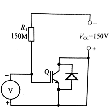
VGES refers to the absolute value of the maximum instantaneous voltage that can be sustained between the gate and emitter. This is an absolute maximum rating and should not be exceeded under any circumstances, otherwise there is a risk of permanent damage.

Simple VGES Test Circuit 1
Most IGBTs have a VGES value of ±20V. VGES emphasizes "survival." This means that even if the value is briefly exceeded, the device may not fail immediately, but its reliability and lifespan will be severely damaged. Sustained exceeding this value will inevitably lead to gate oxide breakdown.
2.2Gate Oxide Breakdown: An Irreversible Disaster
The gate of an IGBT is isolated from the silicon substrate by an extremely thin silicon dioxide (SiO₂) insulating layer. While this dielectric layer has excellent insulation properties, its voltage withstand capability is limited. Once the VGE voltage exceeds VGES, an extremely strong electric field is generated, causing avalanche breakdown in the gate oxide layer. This short circuit or increased leakage between the gate and emitter leads to the IGBT losing its switching control capability, potentially paralyzing the entire IGBT circuit. This is an irreversible physical damage process.

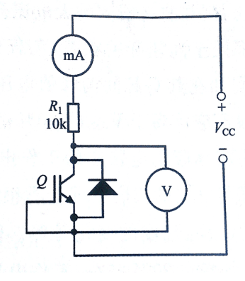
Simple Circuit for Testing VCES 2
3.Relationship between VGE and VGES and Design Key Points
The relationship between them can be understood as follows:
- VGE is the operating voltage you plan and expect to apply (typically +15V/-8V).
- VGES is the voltage ceiling (±20V) that the gate structure can tolerate, a high-voltage line that must never be touched.
In actual IGBT circuit design, to ensure that the transient value of VGE is always lower than VGES, the following measures must be taken:
Precise driver circuit design: Select a dedicated IGBT driver chip or module with stable output and ensure its output level is within the standard range.
Optimize PCB layout: Minimize the length of the driver loop (especially the return path) and reduce parasitic inductance. This is fundamental to suppressing gate voltage overshoot and oscillation. Using a gate resistor (Rg): A series gate resistor is an effective way to suppress current spikes and ringing. However, the value of Rg requires careful consideration (too small a value results in poor suppression, while too large a value increases switching losses).
Using an active Miller clamp: Many modern driver ICs integrate a Miller clamp. When the IGBT is turned off, this function effectively suppresses the gate voltage rise caused by coupling through the Miller capacitance (Cgc), preventing false turn-on and voltage overshoot.
In extreme cases, a TVS diode (transient voltage suppressor) can be connected in parallel between the gate and emitter, with its clamping voltage set slightly below VGES (e.g., 18V) to provide a final measure of gate protection
4.SHYSEMI Recommendations
Whether selecting a discrete IGBT or an integrated IGBT module, the SHYSEMI technical team strongly recommends:
Carefully review the datasheet: Before designing, be sure to confirm the specific VGE(th) and VGES values of the selected device. Allow margin in the driver design: Ensure that even under worst-case operating conditions (such as high temperature and maximum load), the peak voltage of the driver waveform is well below the VGES value.
Verification: Use a high-voltage differential probe to measure the gate waveform on a prototype board to confirm the absence of dangerous overshoot and oscillation.
Conclusion:
Understanding and strictly adhering to the limits of VGE and VGES is essential for every power electronics engineer designing reliable and efficient IGBT circuits. The VGES ±20V barrier is the "safety gate" of the IGBT gate. Maintaining this barrier provides a solid foundation for stable operation of your product.