

Strictly speaking, fully realizing the performance advantages of IGBT devices depends on the optimized design of the driver circuit. A well-designed IGBT gate drive circuit not only improves energy efficiency but also significantly enhances system reliability and stability. SHYSEMI will delve into how to properly drive IGBT modules and IGBT driver design considerations to help engineers avoid common design pitfalls.
1.Optimizing IGBT Gate Drive Voltage
1.1 Relationship between Gate Threshold Voltage and Drive Voltage
Theoretically, an IGBT turns on when the gate-emitter voltage VGE≥VGE(th) (threshold voltage). VGE(th) typically ranges from 5 to 6V. As VGE increases, the IGBT's on-state voltage drop decreases, reducing on-state losses, but also weakening its ability to withstand short-circuit currents. Excessively high VGE can also cause gate voltage oscillations, leading to gate damage.
1.2 Determining the Optimal Drive Voltage
To balance minimizing on-state voltage drop and short-circuit withstand capability, it is recommended to calculate the drive voltage using the formula: VGE ≥ D × VGE(th). When VGE(th) = 6V:
- D = 1.5 → VGE = 9V
- D = 2 → VGE = 12V (optimal value)
- D = 2.5 → VGE = 15V
- D = 3 → VGE = 18V
Typically, the IGBT gate drive voltage should be within the 12-15V range, with 12V being the optimal value. During shutdown, a negative bias of approximately -10V is recommended to improve noise immunity and dv/dt tolerance.
2.IGBT Drive Characteristics Analysis and Optimization
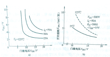
2.1 Impact of Forward Bias Voltage on Performance
Increasing the positive bias voltage, VGE, reduces the on-state voltage and on-state energy dissipation (EON), as shown in Figure 1. When VGE is fixed, the on-state voltage increases with collector current, and conduction losses increase with junction temperature.
a) Relationship between VGE(ON) and VCE
b) Relationship between VGE(ON) and EON
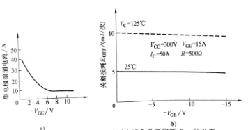
2.2 The Critical Role of Negative Bias Voltage
Negative bias voltage (-VGE) significantly affects the reliable operation of the IGBT. Increasing the negative bias voltage significantly reduces the collector surge current, but has little effect on the turn-off energy dissipation (EOFF).
a) Relationship between -VGE and collector surge current
b) Relationship between -VGE and turn-off energy dissipation (EOFF)
2.3 Optimizing Gate Resistor Design
Increasing gate resistance RG prolongs the IGBT's turn-on and turn-off times, increasing switching losses. Excessively small RG increases di/dt, potentially causing false turn-on and increasing losses across RG.
3.0 Key Considerations in IGBT Drive Circuit Design
3.1 Gate Charge Sensitivity Management
IGBTs have a threshold voltage of 2.5 to 5V and a capacitive input impedance, making them highly sensitive to gate charge. The driver circuit must provide a low-impedance discharge path, and the connection should be as short as possible. The recommended range is 12V ≤ VGE ≤ 18V, and a negative bias voltage of -5V is appropriate.
3.2 Switching Frequency Optimization
Although high-frequency switching can reduce switching losses, it should not be too high under high inductive loads, as this will generate dangerous voltage spikes and may cause device breakdown.
3.3 Gate Resistor and Capacitor Selection
Choosing the appropriate gate series resistor RG and gate-to-emitter capacitor CG is crucial. Too small RG results in excessive turn-on current; too large RG increases switching time and losses. CG helps suppress dic/dt, but too large a value can cause turn-on delay.
3.4 Preventing False Turn-On
When an IGBT is turned off, the gate-to-emitter voltage is susceptible to parasitic interference. It is recommended to connect a parallel resistor between the gate and the emitter, and optionally install two anti-series Zener diodes (with the same voltage as the positive and negative gate voltages).

3.5 Driver Source Characteristics
Use a low-resistance driver to charge and discharge the gate capacitor, ensuring sufficiently steep VGE leading and trailing edges to minimize switching losses. After turn-on, the driver source should provide sufficient power to prevent the IGBT from exiting the saturation region.
3.6 Frequency Response
The driver circuit should be able to effectively transmit pulse signals of tens of kHz.
3.7 Inductive Load Handling
Under highly inductive loads, the IGBT switching time should not be too short to limit the voltage spikes caused by the di/dt transition.
3.8 Electrical Isolation Requirements
Since IGBTs are often used in high-voltage applications, the driver circuit and control circuit must be strictly isolated.
3.9 Protection and Interference Suppression
An ideal IGBT driver circuit should be simple and practical, with built-in protection functions and strong interference suppression capabilities.
Conclusion: Mastering IGBT Driving Techniques Improves System Performance
The characteristics of an IGBT vary significantly with gate drive conditions. Optimizing IGBT driver circuit design requires comprehensive consideration of multiple factors, including gate voltage, resistor configuration, switching frequency, and protection measures. By properly selecting drive parameters (e.g., VGE = 12V, negative bias voltage -5V to -10V) and adhering to the aforementioned design considerations, the efficiency, reliability, and service life of the IGBT can be significantly improved, ensuring optimal performance of the power electronics system.