

In the semiconductor supply chain, transitioning an integrated circuit (IC) from design to mass production requires navigating hundreds of highly challenging fabrication steps. As the backbone of quality control (QC), the semiconductor testing process acts as three rigorous checkpoints that directly determine the reliability of the final delivered silicon. Driven by the continuous expansion of the semiconductor test equipment market, the wafer and package test matrix—comprising WAT (Wafer Acceptance Test), CP (Circuit Probing), and FT(Final Test) —has emerged as a strategic imperative for manufacturers to optimize yield and control manufacturing costs.

SHYSEMI has entered into a partnership with Huahong Group, the sixth largest in the world, and possesses high-precision and comprehensive chip testing and inspection systems. By providing an in-depth analysis of these three core test stages, we aim to help the industry transition from passive inspection to proactive yield management.
1. The Complete IC Test Workflow: Three Checkpoints Working in Synergy
IC testing in semiconductor manufacturing is far more than a simple electrical continuity check. It is a comprehensive quality monitoring and failure analysis (FA) framework spanning the entire lifecycle of wafer fabrication, packaging, and final product delivery. Wafer Acceptance Test (WAT), Circuit Probing (CP), and Final Test (FT) establish sequential defensive lines, forming an IC test network characterized by layered screening and data cross-verification.

[Wafer Fab Complete] -> [WAT: Process Window Monitoring] -> [CP: Wafer-Level Die Sorting] -> [Packaging] -> [FT: Final Product Inspection]
From a manufacturing timeline perspective:
- WAT serves as the post-fabrication "process health check."
- CP handles "wafer-level testing and die sorting" prior to packaging.
- FT acts as the final "product acceptance and delivery gate" post-packaging.
Production data verified by SHYSEMI demonstrates that synchronizing data across these three test stages significantly boosts the overall yield of high-density memory chips and complex SoCs. This synergy drastically reduces defect escape rates prior to packaging, saving design houses and semiconductor foundries up to 30% in wasted packaging costs.
2. WAT: The Process "CT Scan" Before Wafer Gate-Exit
WAT (Wafer Acceptance Test), also known as parametric testing, does not evaluate whether the chip’s internal logic functions correctly. Instead, it measures specific Test Keys or Process Control Monitoring (PCM) structures designed inside the scribe lines. This data evaluates the stability of the front-end semiconductor fabrication process and detects parametric drift across the entire wafer.
2.1 Test Structures and Core Parameters
WAT test structures encompass all foundational semiconductor devices on the process platform, including MOS transistors, diodes, resistors, capacitors, and isolation structures. During process R&D and mass production monitoring, SHYSEMI focuses closely on the following long-tail parametric indicators:
- Transistor Electrical Characteristics: Threshold voltage, saturation current , and subthreshold leakage current.
- Interconnect and Contact Quality: Contact resistance, metal interconnect line resistanc, and via resistance.
- Thin Film and Dielectric Process Monitoring: Sheet resistance, gate oxide thickness, and breakdown voltage.
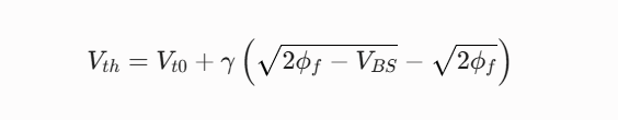
Taking the critical threshold voltageas an example, it is rigorously defined by semiconductor physics as:
2.2 Equipment Precision and Process Engineering Insights
WAT testing demands extreme measurement precision from probe stations and parametric testers, typically requiring a voltage measurement accuracy of ±100nV and a current resolution down to the 10fA level.
For pure-play foundries, WAT data is the sole hard metric used to determine whether a wafer can be released to the next production phase. If WAT parameters drift outside the established process window, it indicates a front-end anomaly—such as ion implantation dosage deviation or non-uniform thin-film deposition. Production lines must be halted immediately for corrective action to prevent the scrapping of entire wafer lots.
3. CP: Wafer-Level Die Sorting Prior to Packaging
CP (Circuit Probing), or wafer testing, is performed before the wafer is diced into individual units. This process utilizes high-precision test adapters (primarily probe cards) to directly interface with the bond pads or bumps on the chip surface, executing full functional and electrical parametric tests on each independent die under active bias.
3.1 Test Platform Architecture and Hardware Challenges
A CP test setup consists of a high-precision prober, a probe card, and Automated Test Equipment (ATE). In scaling up high-density, multi-channel CP testing, SHYSEMI focuses on overcoming several critical technical bottlenecks:
- Signal Integrity and Crosstalk: When dealing with high-speed interface testing or multi-die parallel testing, electromagnetic interference (EMI) between probe tips can severely degrade signal fidelity.
- Contact Resistance (Rc) Control: The contact resistance between the probe tips and chip pads must be stably maintained at ultra-low levels to prevent false failures induced by poor contact or sub-optimal probe-to-pad alignment.
- Multi-Site Test Efficiency: For consumer electronics and IoT silicon, mass production typically deploys 64-site or higher parallel testing. This places stringent demands on the power channel and digital instrument response times of the ATE system.

3.2 Test Coverage and Wafer Repair
CP testing primarily focuses on:
- Static and Dynamic Electrical Parameters: Leakage current, power consumption, ON-resistance, and I/O voltage levels.
- Structural Functional Verification: Executing scan chain tests (Scan) and Memory Built-In Self-Test (BIST).
- Long-Tail Application Scenarios: High/low-frequency trimming (Trim) and OTP/EEPROM programming and verification.
For memory devices such as SRAM, DRAM, or Flash, CP testing also handles redundancy repair. By deploying laser fuses or electronic fuses (E-fuses), defective memory cells are swapped out for spare on-chip units—a core method for maximizing wafer test yields. Upon completion, the system generates a precise Wafer Map that flags bad dies, instructing subsequent die-bonding and packaging lines to reject defective silicon.
4. FT: The Ultimate Examination for Packaged ICs
FT (Final Test) is the definitive, 100% inspection gate before integrated circuits exit the factory. Conducted after packaging is complete, FT simulates ambient, high-temperature, or low-temperature operating environments to validate the electrical performance and logic functionality of the device under realistic application workloads.
4.1 Final Test Systems and Environmental Stress Simulation
An FT system mainly comprises an ATE system, an automated handler, and a dedicated test socket. The handler precisely routes packaged devices into the test socket, where the ATE injects stimulus signals and captures the output responses.
To guarantee the long-term reliability of automotive-grade and industrial-grade ICs in extreme environments, FT protocols typically enforce a rigorous tri-temperature test flow (cold testing at -40°C, ambient testing at 25°C, and hot testing at 125°C to 150°C).
For missions where high reliability is non-negotiable, devices must undergo Highly Accelerated Stress Testing (HAST) and High-Temperature Operating Life (HTOL) burn-in screening. This ensures early infant mortality failures—the initial phase of the reliability bathtub curve—are completely eliminated.

4.2 Core FT Test Disciplines
- Full Functional Fault Coverage: Running comprehensive system-level test vectors to ensure 100% coverage of logical peripherals, co-processors, and computing cores.
- RF and High-Speed Signal Testing: Performing eye diagram testing, jitter analysis, and Bit Error Rate (BER) testing for RF silicon (5G, Wi-Fi) and high-speed SerDes interfaces.
- ESD and Overvoltage Qualification: Verifying Electrostatic Discharge (ESD) protection ratings and latch-up immunity.
5. Key Differences: WAT vs. CP vs. FT
To provide a clear view of where these methodologies sit within the broader IC test landscape, SHYSEMI has synthesized the core technical dimensions below:
6. Strategic Value of High-Efficiency Testing Across the Semiconductor Supply Chain
In the More-than-Moore era, dominated by advanced packaging techniques like Chiplets and 3D stacking, semiconductor testing has evolved from a passive quality gate into a full-lifecycle yield control hub. By implementing digitalized volume production management, SHYSEMI's engineer has demonstrated that connecting WAT, CP, and FT test data across a unified Yield Management System (YMS) unlocks massive statistical data synergy:
- Closed-Loop Failure Traceability: If a specific frequency band exhibits signal attenuation during FT, engineers can trace the data stream back to the parametric distribution at CP, or even map it to a micron-level deviation in sheet resistance recorded during WAT. This cross-stage failure analysis allows process engineers to isolate root causes in record time.
- Test Coverage Optimization and Cost Balancing: Blindly targeting 100% test fault coverage at the FT stage causes test costs to skyrocket exponentially. SHYSEMI advocates shifting specific functional blocks left into the CP phase, or dynamically adjusting FT sampling strategies based on the robustness of the WAT process window. This maintains a strict Zero Defect delivery standard while optimizing test economics.

SHYSEMI also offers chip design and tape-out services. Let's get started.send a eamil:info@shysemi.com
As IC integration scales across generations, invisible test boundaries continuously safeguard the electrical pulse of every silicon wafer. From micron-scale wafer test keys to high-speed packaged devices with thousands of pins, it is the rigorous pursuit of advanced WAT, CP, and FT technologies that enables high-quality semiconductor products to successfully transition to the global marketplace.