

Introduction
With the rapid evolution of silicon carbide (SiC) MOSFET technology, its high-frequency switching advantages over traditional Si IGBTs have attracted increasing attention from engineers.This advantage primarily stems from the high electron saturation drift velocity of SiC MOS devices, enabling rapid transitions between on and off states, significantly reducing switching time.
At the same time, as a unipolar device, SiC MOSFETs exhibit no minority carrier storage during freewheeling, unlike bipolar Si IGBTs. This results in dramatically lower reverse recovery losses. In fact, the reverse recovery charge (Qrr) of SiC MOS is typically only about one-tenth that of comparable silicon devices.

In many applications, such as: motor drives, EV charging, solar inverters, the intrinsic body diode of the SiC MOSFET can be directly used as the freewheeling diode, improving power density while reducing system cost.
To fully exploit these high-frequency capabilities, the industry has adopted Double Pulse Testing (DPT) as the standard for evaluating dynamic characteristics. But what exactly constitutes a DPT platform?

Figure 1. Topology of the dual-pulse testing circuit
A standard half-bridge inductive load DPT setup consists of:
- DC bus supply (VBUS)
- DC link capacitor (CBUS)
- Load inductor (LLoad)
- Device under test (DUT) and auxiliary switch
- Gate driver (VG) and gate resistor (RG)
- Current probe (Rogowski coil or coaxial shunt)
- Parasitic inductances from layout and components
In practice, the upper switch is typically used as a freewheeling device, while the lower switch (DUT) is actively driven.
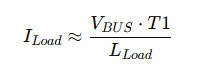
During testing, two pulses are applied:
- The first pulse (T1) builds up load current:
- The second pulse is used to evaluate switching behavior
Engineers primarily analyze:
- Turn-off waveform during the first pulse
- Turn-on waveform during the second pulse
Key Technical Considerations in SiC MOS Double Pulse Testing
1. Probe Timing Skew
Accurate measurement requires synchronization between:
- Gate voltage (VG)
- Drain-source voltage (Vds)
- Current waveform
While voltage probes can be calibrated relatively easily, timing mismatch between current and voltage probes (typically a few to tens of nanoseconds) can introduce significant errors in switching energy calculations.
For example, a 10 ns timing offset can dramatically alter measured switching losses (Eon/Eoff). Proper calibration—aligning the gate threshold crossing with current rise—is essential.

Figure 2. The process of turning on the device

Figure 3. Device shutdown process
Key takeaway:
Even nanosecond-level misalignment can distort results. Regular probe calibration is mandatory.
2. Gate Resistor Selection (Rg)
Gate resistance has a critical impact on switching performance.
Datasheets often specify low Rg values (e.g., ~2Ω) to demonstrate minimal switching loss. However, such values are often impractical in real applications.
2.1 Lower Rg:
- Faster switching
- Lower switching loss
- Higher di/dt → increased current overshoot
2.2 Higher Rg:
- Reduced overshoot
- Improved stability
- Increased switching loss
For example:
- Rg = 2.4Ω → lower loss but current overshoot up to 3× rated current
- Rg = 20Ω → reduced overshoot but significantly higher losses
Design trade-off:
Balance switching efficiency and device reliability based on application requirements.
3. Parasitic Inductance Management
Parasitic inductance—often underestimated—has a major impact on switching behavior.
It originates from both:
- Test circuit layout
- Device packaging (especially source inductance)
In packages like TO-247-3L, common source inductance introduces voltage fluctuations that slow switching speed.
In contrast, TO-247-4L (Kelvin source) design minimizes this effect by separating the gate return path, reducing switching losses.
The influence of TO-247-4L pin pair on dual pulse test:

The opening process of the dual-pulse test device in the TO-247-3L package

TO-247-3L package dual pulse test device shutdown process
Experimental results show:
- Poor mounting or incomplete pin insertion increases parasitic inductance
- Even a ~9 nH difference can significantly increase switching losses
To further minimize parasitics, surface-mount packages such as TOLL are recommended.
Key takeaway:
Layout and mounting consistency are essential for accurate and repeatable test results.
Summary
Double Pulse Testing is a powerful and essential method for accurately evaluating the dynamic switching performance of SiC MOSFETs.
However, relying solely on datasheet values is insufficient. Engineers must carefully consider:
- Probe calibration
- Gate resistance selection
- Parasitic inductance control
These factors are critical for obtaining reliable and application-relevant performance data.
If you have questions regarding SiC device selection, circuit design, or parameter optimization, SHYSEMI’s engineering team is ready to provide one-on-one technical support and tailored solutions.
SHYSEMI recommends a product model that has already been tested in the market:
- Package: TO-247-3L
- Voltage Rating: 1200V
- RDS(on) (typ.): 30mΩ
Typical Applications
- Solar inverters
- Switched-mode power supplies (SMPS)
- High-voltage DC/DC converters
- Battery chargers
- Motor drives
- Pulsed power systems
- Welding equipment
- EV charging
Key Features
- Fast intrinsic diode with ultra-low reverse recovery (Qrr)
- Halogen-free and RoHS compliant