

Ever since Tesla's third-generation electric drive system integrated mass-produced TPAK SiC modules—achieving breakthroughs in both vehicle efficiency and power density—domestic power semiconductor packaging companies, OEMs, and tier-1 electric drive solution providers have accelerated their development of the TPAK single-switch power packaging roadmap.
Leveraging SHYSEMI's proprietary TPAK SiC module line, this article provides a systematic analysis of the core technical advantages and implementation strategies of this packaging architecture in automotive traction inverters. The following analysis focuses on SHYSEMI's TPAK-packaged SiC modules specifically engineered for on-board chargers (OBC) and main traction inverters.

Real photo of the SiC module with TPAK packaging for OBC application from SHYSEMI
1. TPAK vs. TO-247 Packaging Topologies: Core Advantages
The TPAK belongs to the single-switch module category, positioned strategically between standard discrete power transistors and multi-chip power modules. This architecture successfully eliminates the common pain points of traditional TO-247 discrete devices—such as high parasitic inductance, restricted continuous output current, and poor current sharing during multi-tube paralleling—while retaining the scalability of modular paralleling.
Designers can flexibly scale the number of paralleled TPAK SiC or TPAK IGBT modules based on the inverter's rated power and peak output requirements. This platform-based scalability allows a single inverter design to adapt to the complete electric powertrain range (75 kW to 300 kW) for passenger and commercial vehicles.

Table 1: Stray Inductance & Electrical Parameters Comparison of Mainstream Power Packages
Package stray inductance simulation data demonstrates that the TPAK package significantly reduces stray inductance compared to traditional TO-247 discrete packages, leading to a dramatic boost in continuous current-carrying capacity. Lower parasitic inductance allows the system to utilize TPAK SiC chips with lower turn-off gate resistance (Rg,off). This effectively suppresses turn-off voltage spikes, decreases switching losses (Ets), minimizes die temperature rise, and broadens the module's continuous output current envelope.
Thermal Simulation Test Conditions: DC link voltage = 410V, output RMS current = 260 Arms. Utilizing SHYSEMI's single-row TPAK SiC die layout, the steady-state junction temperature (Tj) of the die is approximately 132℃. This sits well below the 150℃ maximum automotive operating junction temperature threshold, demonstrating excellent continuous load capacity and liquid-cooling thermal performance.

Figure 1 Thermal simulation results of the TPAK single-module single-row configuration for current carrying capacity
2. SHYSEMI TPAK Die Layout: Achieving SiC Cost Reduction & IGBT Universal Design
The internal die configuration of the TPAK package offers exceptional flexibility: it can accommodate 2 paralleled SiC MOSFET dies or a single integrated 300A/400A silicon-based IGBT wafer.
To address the high raw material costs of SiC substrates, SHYSEMI's TPAK SiC module utilizes a modularized decomposition layout. This design minimizes the total SiC chip surface area required per inverter while maintaining equivalent power output, effectively controlling system Bill of Materials (BOM) costs. Concurrently, the mechanical package dimensions and pinout definitions are 100% compatible with silicon-based TPAK IGBTs. This allows a single traction inverter hardware layout to seamlessly alternate between SiC and IGBT power configurations, offering unparalleled platform reuse.

Figure 2 Internal chip layout structure diagram of TPAK packaged IGBT/SiC
3. High Automotive Reliability via TPAK Structure & Packaging Materials
Whether deployed in mass-produced Tesla inverters or in next-generation 400V/800V powertrains currently under development by automotive OEMs, the TPAK package offers three structural advantages over traditional full-bridge modules:
- Higher system power density
- A highly compact structural envelope
- Exceptional mechanical vibration resistance
This makes it an ideal fit for the confined spaces of automotive front bays and harsh vehicle vibration conditions.
This premium performance stems directly from advancements in packaging materials and interconnect technologies:
- AMB (Active Metal Brazing) Ceramic Substrates: TPAK utilizes AMB ceramic substrates paired with Cu-Clip (Copper Clip) interconnects, entirely replacing traditional aluminum wire bonding.
- Elimination of Wire Bonding: This eliminates the risk of wire liftoff, drastically reduces parasitic parameters, optimizes module thermal resistance (Rth,jc), and increases current carrying density.

Figure 3 Schematic diagram of the internal AMB ceramic substrate + Cu-Clip copper clip structure in TPAK
SHYSEMI has successfully achieved volume production of automotive-grade TPAK packages. A flagship specification is our 1200V/230A TPAK SiC module, featuring a maximum on-resistance (RDS(on),max) of 12Ω. This TPAK SiC product line covers two core automotive applications: EV main traction inverters and high-voltage, high-power On-Board Charger (OBC) systems. We have established long-term strategic partnerships with leading global automakers, including Volkswagen, BAIC, and GAC.
4. Advanced Laser Welding Process: Minimizing Contact Resistance and Stray Inductance
To further reduce contact resistance and stray inductance in the main power loop, all TPAK power output terminals are constructed from high-conductivity copper substrates and interconnected using Copper-to-Copper (Cu-Cu) laser welding.
This process, already mature within EV power battery cell terminal welding, creates a homogeneous copper-to-copper interface with high mechanical bonding strength and stable thermal/electrical conductivity. It effectively prevents interface oxidation and impedance drift after extensive thermal cycling and vibration aging, establishing itself as the dominant interconnect technology for automotive power modules.
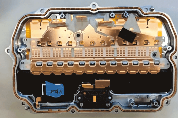
Figure 5. Schematic diagram of laser welding of copper terminals of Tesla electric drive system TPAK module.
5. Three-Phase Full-Bridge Inverter Layouts: Supporting Single and Dual Motor Integrated Systems
For three-phase full-bridge motor controller topologies, the TPAK module architecture is primarily deployed in two parallel configurations:
Single-Row Die Layout
Mainly utilized in low-to-medium-power inverters, this layout directly serves as a pin-to-pin alternative to traditional standard HP1 (300A/400A) power modules. Its streamlined structure simplifies die welding and final system assembly, resulting in total BOM and manufacturing costs that are lower than those of an HP1 module.

Figure 6 Layout diagram of TPAK module single/multi-tube parallel structure
Multi-Module Dual-Row Parallel Configuration
Engineered for high-power 800V high-voltage platforms, this hardware configuration supports the parallel expansion of up to four TPAK SiC/IGBT modules per switch. The number of paralleled modules can be dynamically scaled based on the vehicle's peak power requirements without redesigning the gate driver board or main control circuitry. This drastically reduces customer product development cycles and minimizes hardware/software NPI engineering costs.
Simultaneously, the compact footprint and superior power density of the TPAK package provide ample design space for mainstream dual-motor integrated systems. Paralleled TPAK modules can be mounted on both sides of a dual-sided water-cooled channel, enabling integrated dual-motor drive architectures that compress the overall powertrain volume and shorten vehicle wiring harness lengths.
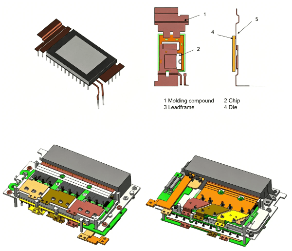
Figure 7. Dual-electric integrated water-cooling layout scheme based on TPAK SiC module
Conclusion
The TPAK single-switch package has become the mainstream power semiconductor architecture for next-generation electric powertrains due to its four core advantages:
- Ultra-low stray inductance
- Flexible parallel scalability
- High power density
- Strict automotive-grade reliability
SHYSEMI’s mass-produced, highly reliable TPAK SiC modules provide a complete reference solution for automotive OEMs, electric drive developers, and OSAT companies. This makes SHYSEMI the premier Chinese power module manufacturer for next-generation, lightweight EV motor control systems.

For a quote and more information, just click the email address:info@shysemi.com
Industrial FAQ: TPAK SiC Module Automotive Applications
Q1: What are the reliability advantages of the TPAK package utilizing AMB substrates and Cu-Clip technology over traditional aluminum wire-bonded modules?
A1: Traditional aluminum wire bonds are highly susceptible to fatigue cracking and interface resistance degradation under harsh automotive thermal cycling (-40℃ - 150℃). The Cu-Clip covers a much larger area of the die surface, yielding lower thermal resistance and superior current sharing. Paired with an AMB ceramic substrate, it offers enhanced resistance to thermal shock, doubling the power cycling lifetime and perfectly matching the high-temperature operating characteristics of SiC chips.
Q2: Can the SHYSEMI 230A TPAK SiC module operate continuously at 260 Arms under a 410V DC link voltage condition?
A2: Yes. Thermal simulations confirm that the steady-state junction temperature of the single-row layout under these conditions is approximately 132℃, well below the 150℃ automotive operating limit. When paired with an optimized liquid cooling system, it can reliably deliver a continuous 260Arms output current with ample margin for short-term peak currents, making it ideal for mainstream 400V passenger EV traction drives.
Q3: Aside from main traction inverters, what other automotive applications can benefit from TPAK SiC modules?
A3: The SHYSEMI TPAK SiC series is fully compatible with high-voltage On-Board Chargers (OBC), DC-DC boost modules, and auxiliary drives for commercial vehicles. The 1200V voltage-rated specifications are also ideally suited for 800V high-voltage fast-charging platforms, allowing OEMs to achieve single-package platform standardization across multiple vehicle sub-systems.