

The 600V–650V voltage node has become the ultimate battleground for high-frequency, high-efficiency, and high-power-density power electronics design. Today, three distinct technologies dominate this space: Silicon Superjunction MOSFETs (Si SJ MOS), Silicon Carbide MOSFETs (SiC MOS), and Gallium Nitride High Electron Mobility Transistors (GaN HEMT).
To give you a precise, data-backed selection guide for your next high-frequency power supply, energy storage system, or industrial motor drive, SHYSEMI cross-evaluated the latest device platforms from top-tier global manufacturers, including Infineon, STMicroelectronics, onsemi, and Toshiba. Here is how they stack up.

1. Device Architecture and Physical Foundation
The root of all performance differences lies under the hood. The physical layout and material properties of these three devices dictate how they behave under real-world operating conditions.
1.1 Si SJ MOS (Silicon Superjunction)
A mature, vertical structure where the source and drain are located on opposite sides of the die. It relies on alternating, tightly controlled P-and-N pillars to achieve charge compensation.
The Benefit: This architecture shatters the historic "silicon limit" for specific on-resistance. Today's market is split between two proven manufacturing approaches: multi-layer epitaxy (pioneered by platforms like Infineon's CM8) and deep trench technology (championed by platforms like Toshiba's DTMOS VI).
1.2 SiC MOS (Silicon Carbide)
Also a vertical structure, utilizing either planar layouts (e.g., onsemi M3S, ST G3) or trench geometries (e.g., Infineon M2H).
The Benefit: Thanks to the wide-bandgap properties of SiC, these devices simultaneously deliver high-frequency switching and excellent high-voltage blocking capabilities.
1.3 GaN HEMT (Gallium Nitride)
A fundamentally different, lateral architecture where the source, drain, and gate terminals sit entirely on the top layer of the chip. Because GaN cannot grow high-quality native thermal oxides, the industry heavily relies on p-GaN enhancement-mode (E-mode) structures like Schottky Gate Transistors (SGT) or Gate Injection Transistors (GIT).
1.4 The Structural Catch
GaN HEMTs lack a native body diode, giving them the unique potential for bidirectional channel conduction and bidirectional voltage blocking. However, because there is no traditional P-N junction, GaN devices cannot tolerate avalanche breakdown. To counter this, manufacturers build in massive voltage margins—a nominal 650V GaN HEMT typically boasts an actual breakdown voltage exceeding 800V to clear headroom for voltage transients.
2. Key Static Parameters and Thermal Stability
While all three devices operate through standard cutoff, linear, and saturation regions via gate capacitance charging, their static electrical baselines tell very different stories.
2.1 Gate Threshold (VGS(th)) and Drive Requirements
- Si SJ MOS: Features a comfortable (VGS(th) between 3.0V and 4.5V and typically recommends a 10V to 15V gate drive. It uses the most mature, plug-and-play gate drive ecosystem available.
- SiC MOS: Planar types sit around 2.7V to 3.0V, while trench architectures land closer to 4.0V to 4.5V. They typically require a +18V turn-on drive (with backward compatibility to 15V). The Benefit: Its drive characteristics closely mirror traditional silicon, ensuring the lowest platform migration cost for engineering teams transitioning from Si IGBTs or SJ MOS.
- GaN HEMT: Operates on a razor-thin margin. The GIT structure triggers around 1.2V, while the SGT structure triggers around 1.7V, requiring a nominal drive voltage of just 3V to 6V. The Design Impact: While this allows for blistering switching speeds, the incredibly low threshold leaves the device highly sensitive to gate noise and parasitic ringing. Your PCB layout and gate driver loop design must be absolutely flawless.
2.2 RDS(on) Thermal Stability
Power devices rarely run at room temperature. Evaluating how on-resistance degrades at high junction temperatures is critical for realistic thermal management.
SiC MOS is the clear winner: At 150°C, its RDS(on) temperature coefficient is an astonishingly low 1.2 to 1.5, with a maximum rated junction temperature (Tj) of 175°C. Why this matters: In hot, tightly packed enclosures, a SiC MOS maintains low conduction losses. This allows you to relax your cooling constraints or down-size your device. For instance, a 50–60mΩ SiC MOS can often replace a 30–40mΩ Si SJ MOS or GaN HEMT under hot operating conditions.
Si SJ MOS and GaN HEMT: Both exhibit a much steeper curve, with temperature coefficients between 2.1 and 2.5 at 150°C. Their on-resistance more than doubles when hot, and their maximum Tj is strictly capped at 150°C.

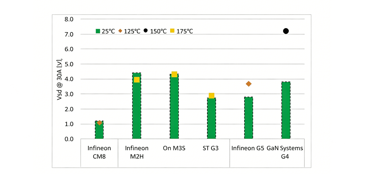
2.3 Reverse Conduction Voltage Drop VSD
Si SJ MOS: Its inherent body diode delivers a forward drop VSD around 1V, making it highly efficient during dead-time freewheeling.
SiC MOS and GaN HEMT: Both suffer from a high reverse voltage drop. SiC sits between 3.0V and 4.5V. GaN HEMTs operate via reverse channel conduction rather than a physical diode; depending on your negative gate turn-off voltage, this drop can range from 3V to 4V at room temperature and degrade to 4V to 7V at high temperatures. To prevent severe freewheeling losses, implementing aggressive Synchronous Rectification (SR) is highly recommended.
3. Dynamic Switching Performance
Switching speed is entirely a function of how fast your gate drive can charge and discharge the device’s internal parasitic capacitances (Ciss, Coss, Crss).
[Switching Performance Hierarchy]
GaN HEMT ──────► Lowest Qg, Zero Minority Carriers (Qbip=0), Lowest Loss
SiC MOS ──────► Low Qg, Negligible Minority Carriers (<5%), GaN-Like Speed
Si SJ MOS ──────► High Qg, High Qoss & Qrr, Significant Switching Penalty
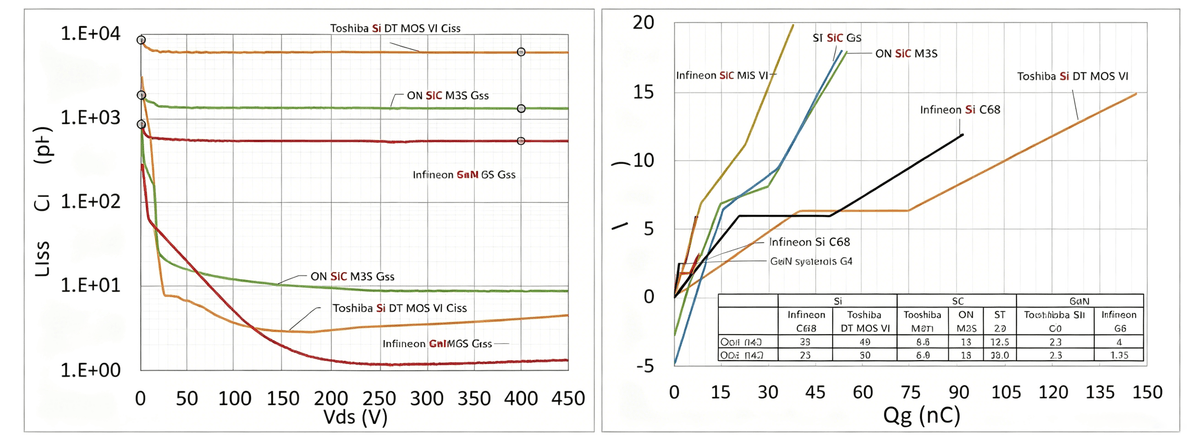
3.1 Gate charge (Qg) and Input Capacitance
Across the entire voltage range, GaN HEMTs offer the lowest Ciss and Qg in the industry. Its gate-source charge (Qgs) is roughly 1.3nC—nearly 1/20th that of a Silicon Superjunction device. The Benefit: Gate drive losses drop to next to nothing, and switching times plunge into the picosecond/nanosecond realm. SiC MOS follows closely behind, while Si SJ MOS demands a massive Qgs (21nC to 40nC), capping its maximum efficient switching frequency.
3.2 Output Capacitance (Eoss / Qoss) and Reverse Recovery (Qrr)
The Si SJ MOS Bottleneck: Even with optimized fast-recovery body diodes, a Silicon Superjunction's Coss at low voltage (0V - 30V) is a full order of magnitude larger than its wide-bandgap rivals. Worse yet, its reverse recovery charge (Qrr) is heavily plagued by minority carrier storage (Qbip accounts for 30% to 44% of the total charge). In high-frequency hard-switching topologies, this triggers harsh current spikes and massive turn-on losses.
The WBG Advantage: SiC MOS and GaN HEMT cut Qrr by more than 10x compared to silicon. Because GaN HEMTs lack a minority-carrier-based physical diode, their Qbip is natively zero. SiC MOS limits Qbip to less than 5%. The Benefit: Both wide-bandgap devices run beautifully in both hard-switching (like Totem-Pole PFC) and soft-switching (like LLC) architectures with minimal energy penalties.
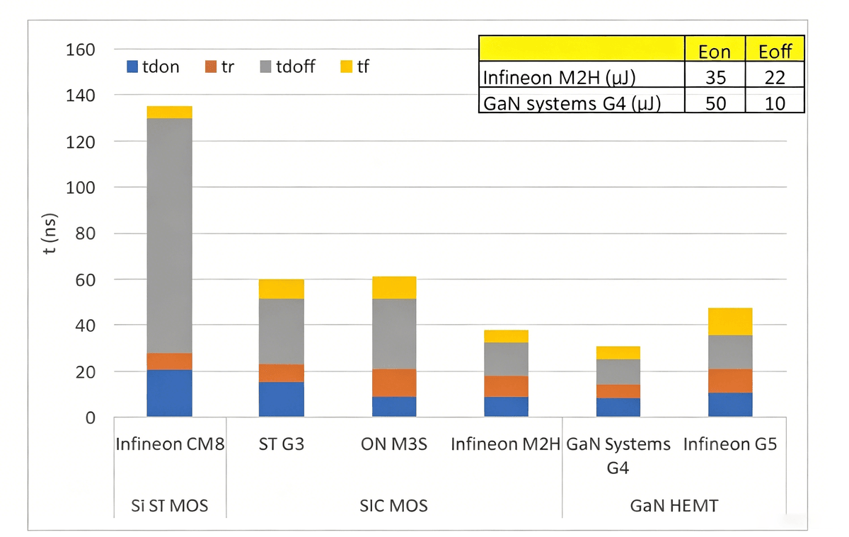
3.3 Real-World Switching Speeds
When housed in advanced, low-parasitic TOLL (TO-Leadless) packaging, both SiC MOS and GaN HEMT compress their actual switching times to a mere 30ns to 60ns. Platforms like Infineon’s M2H (SiC) and GaN Systems’ G4 (GaN) deliver nearly identical ultra-low switching losses, leaving legacy silicon far behind.
4. Engineering Selection and Application Mapping
To help you map these findings to your system requirements, SHYSEMI categorizes the optimal application boundaries for each technology:
Si SJ MOS: The Cost-to-Performance Workhorse
- Optimal Fit: Low-to-medium frequency, cost-sensitive power designs.
- Key Benefits: Highest maturity, lowest bill-of-materials (BOM) cost, excellent low reverse-conduction drop, and zero gate-drive redesign overhead.
- Real-World Applications: Major home appliances, consumer electronics adapters, and standard industrial raw switching power supplies.
SiC MOS: The High-Reliability, High-Power Density Flagship
- Optimal Fit: High-frequency, high-efficiency systems running under harsh thermal and high-power conditions.
- Key Benefits: Elite thermal stability (175℃ rating, flat RDS(on) curve) combined with excellent ruggedness. It serves as a seamless performance upgrade path from silicon in complex soft- or hard-switching circuits.
- Real-World Applications: Electric vehicle onboard chargers (OBC), solar central/string inverters, and industrial energy storage PCS units. As a trusted Chinese manufacturer, SHYSEMI’s SiC MOS solutions are fully market-proven in automotive and photovoltaic inverter fields through long-term partnerships with leading global enterprises.
GaN HEMT: The Ultra-High Frequency Pinnacle
- Optimal Fit: Low-to-medium power applications demanding absolute minimalism, zero weight, and extreme switching frequencies.
- Key Benefits: Near-ideal Qg and Qrr profiles enabling MHz-level switching speeds.
- Real-World Applications: Ultra-compact consumer PD fast chargers, ultra-efficient hyperscale server power supplies, and high-frequency solar micro-inverters.
- The Next Frontier: Because its lateral layout concentrates heat on the top of the die, thermal management remains the primary constraint. Overcoming this thermal bottleneck to scale into higher kilowatt ranges is the next major focus for GaN technology.

For any questions or product inquiries, please contact us via email or WhatsApp:+86 15361554542
Technical Selection FAQ
Q1: Since GaN HEMT delivers the best high-frequency performance, will it completely wipe out Si SJ MOS and SiC MOS at 650V?
SHYSEMI: No. These three technologies will coexist for a long time because they target different engineering priorities.
Si SJ MOS will hold its ground in cost-critical, low-to-medium frequency consumer designs.
SiC MOS remains the king of high-power handling (typically above 3kW). Its vertical structure handles thermal dissipation far better than lateral GaN, making it irreplaceable in rugged environments like automotive traction or heavy energy storage.
GaN HEMT will dominate the sub-3kW space where shrinking the physical footprint via ultra-high frequency operation provides the highest system value.
Q2: Can I drop a SiC MOS directly into my existing Si SJ MOS gate drive circuit?
SHYSEMI: Absolutely not. Doing so will likely under-drive or damage the device.
Legacy Si SJ MOS operates comfortably with a +10V to +15V rail and turns off safely at 0V.
To minimize conduction losses, a SiC MOS requires a much harder push—typically a +15V to +20V turn-on voltage. Furthermore, because high-frequency switching induces massive dv/dt transients, you need a negative turn-off voltage (typically -3V to -5V) to prevent parasitic, accidental re-triggering. You must redesign the bias rails and use a dedicated SiC gate driver.
Q3: What exactly do "bidirectional conduction" and "bidirectional blocking" mean for GaN HEMTs?
SHYSEMI: Bidirectional Conduction: Because a GaN HEMT lacks a true physical P-N body diode, electricity can flow backward from source to drain right through the primary electron channel when the gate is open. Best of all, it does this with zero reverse recovery charge (Qrr=0), which makes it a dream component for synchronous rectification.
Bidirectional Blocking: Standard MOSFETs can only block voltage in one direction because their internal body diode will forward-bias and conduct if the polarity flips. Since GaN has no native body diode, specialized monolithic "Dual-Gate" GaN designs can block voltages coming from both the forward and reverse directions on a single chip.
The Engineering Payoff: This allows you to radically simplify bi-directional topologies like Matrix Converters or T-type three-level bi-directional inverters. You can slash your component count, shrink your footprint, and remove significant conduction bottlenecks from your system.