

In motor drives, solar inverters, energy storage systems (ESS PCS), UPS, and industrial power supplies, dead time is a critical control system parameter.
An optimal dead time protects power devices like IGBTs and MOSFETs from catastrophic shoot-through failures. However, an improperly configured dead time distorts the output waveform, lowers efficiency, and degrades control accuracy. Balancing dead time is essential for power electronics optimization.
At SHYSEMI, a specialist in power semiconductor R&D, we carefully balance device switching characteristics and dead-time control strategies. Our advanced IGBT modules, Intelligent Power Modules (IPMs), and motor drive solutions help clients maximize system reliability and conversion efficiency.
What is Inverter Dead Time?
Dead time (also known as interlocking time) is a brief delay blanking period intentionally inserted by the controller when switching between the upper and lower power switches (IGBTs, MOSFETs, etc.) of the same phase leg.
Consider a standard half-bridge inverter setup:
- When the upper switch (T1) turns off, the controller does not turn on the lower switch (T4) immediately.
- The controller waits for a microscopic delay Δt before triggering T4.
- The same delay applies during reverse switching.
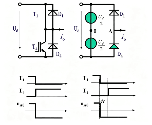
The sole purpose of this delay is to prevent shoot-through. Without dead time, switching delays could cause both switches to conduct simultaneously, short-circuiting the DC bus and instantly destroying the power devices. Because all IGBTs and MOSFETs exhibit turn-on and turn-off delays, dead time is an indispensable protection feature in inverter design.
6 Key Impacts of Dead Time on Inverter Performance
While dead time ensures system safety, it introduces unwanted side effects to inverter performance.
1. Output Voltage Waveform Distortion
During the dead-time interval, both switches are turned off. The output voltage is dictated by the freewheeling path rather than the PWM control signal, leading to:
- Shortened output voltage pulses.
- SPWM waveform distortion.
- Increased Total Harmonic Distortion (THD), which places a heavier burden on filtering components.
2. Reduced Output Voltage
Every PWM cycle loses a fraction of its effective output time, effectively reducing the modulation depth. This causes:
- A drop in fundamental voltage amplitude.
- Lower voltage utilization.
- Degraded output capacity under high-power loads.
3. Zero-Crossing Distortion
The dead-time effect is most pronounced around the current zero-crossing point. For applications like servo drives, variable frequency drives (VFDs), and EV traction motors, this causes:
- Current waveform distortion.
- Torque ripple.
- Degraded low-speed performance.
4. Phase Errors
Dead time causes the output fundamental wave to lag behind the reference signal. In grid-tied inverters or high-precision motor control systems, this compromises:
- Power factor control.
- Current loop control accuracy.
- Grid synchronization performance.
5. Decreased Conversion Efficiency
During dead time, the load current typically flows through freewheeling diodes. Because diode conduction generates extra losses, systems experience:
- Higher conduction losses.
- Increased thermal dissipation.
- A slight drop in overall system efficiency.
6. Elevated EMI
- High-frequency harmonics generated by waveform distortion increase:
- Electromagnetic radiation.
- Conducted interference.
The overall complexity of EMC compliance design.
Dead-Time Analysis in Voltage Source Inverters (VSI)
When both the upper and lower switches are turned off, the load current does not stop instantly; it continues via the freewheeling diodes. The exact circuit behavior depends on the direction of the current.
Scenario 1: T1 to T4 switching (Current flowing OUT of the inverter)
Initially, T1 conducts. When T1 turns off and the circuit enters dead time, the load current automatically freewheels through diode D4. Even when the controller sends the turn-on signal to T4, T4 does not immediately carry the current because the freewheeling path remains unchanged. Consequently, there is no diode reverse recovery and no significant recovery current.
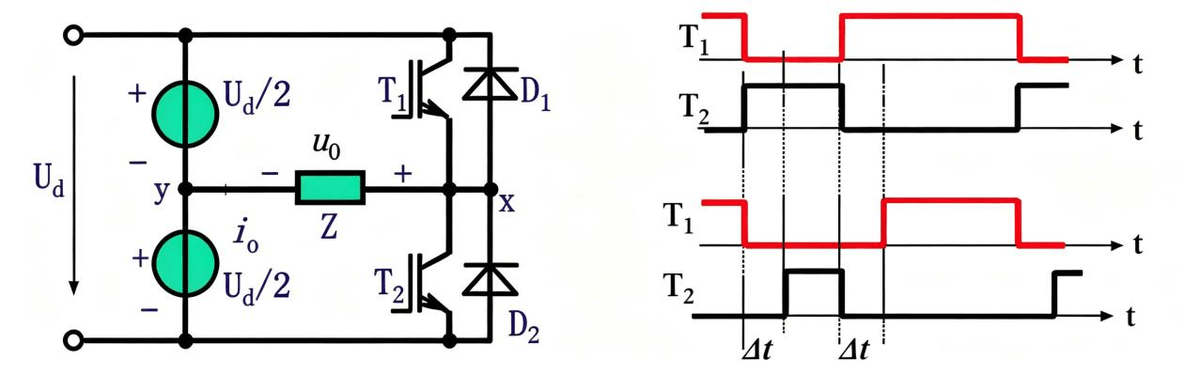
Scenario 2: T1 to T4 switching (Current flowing INTO the inverter)
Initially, diode D1 handles the freewheeling current. During dead time, the current continues through D1. However, when T4 turns on, D1 must shut down rapidly. Due to the diode's reverse recovery time (t_rr), both D1 and T4 conduct simultaneously for a brief moment. This phenomenon creates massive:
- Reverse recovery currents.
- Current spikes.
- Voltage spikes.
If the power devices or gate drivers are poorly matched, this increases phase-leg stress and jeopardizes system reliability. This is why modern high-performance inverters increasingly rely on Fast Recovery Diodes (FRDs), SiC Schottky diodes, and low-reverse-recovery IGBT/IPM modules.
Typical Dead Time Values by Device Type
While safety is a priority, a larger dead time is not always better. It must be optimized based on switching speed, gate drive capability, and PWM frequency.
Common Dead-Time Compensation Techniques
To mitigate the performance drawbacks of dead time, engineers implement several compensation strategies:
- Pulse-Width Compensation: Adjusts the PWM pulse width based on real-time current direction.
- Average Voltage Compensation: Calculates the average voltage error caused by dead time and offsets it in the control loop.
- SVPWM Dead-Time Compensation: Modifies vector duration within Space Vector Pulse Width Modulation algorithms.
- Advanced Control Algorithms: Utilizes high-performance gate drivers and adaptive control algorithms to minimize dead-time errors and boost system efficiency.
Conclusion
Dead time is a non-negotiable safety mechanism for reliable inverter operation, preventing catastrophic shoot-through and safeguarding IGBTs and MOSFETs. However, it introduces trade-offs like waveform distortion, lower efficiency, higher EMI, and reduced &control accuracy.
Optimizing modern inverter systems requires a holistic approach that combines proper dead-time configuration, high-performance power devices, robust gate drive circuits, and smart compensation algorithms.
SHYSEMI provides a comprehensive lineup of IGBT modules, Intelligent Power Modules (IPMs), and power semiconductor solutions. We are dedicated to helping our clients achieve the ultimate balance of reliability, efficiency, and precision control across industrial drives, renewable energy, and motor control applications.

For product information or technical support, please send us an email:info@shysemi.com, or add us on WhatsApp: +86 15361554542